A high-κ homogeneous printable ink and ACEL devices
As illustrated in Fig. 1a, the primary components of the printable high-κ, high-transparency homogeneous ink comprise Polyurethane acrylate (PUA) and 4-acryloylmorpholine (ACMO), which undergo polymerization and curing under UV light to form a robust polymer network. The simultaneous inclusion of ACMO and PUA is a deliberate design choice based on a comprehensive consideration of viscosity and dielectric loss. We found that excessive viscosity significantly deteriorates the patterning precision during screen printing. If ACMO is excluded and only PUA and PC are used, a substantially higher PC content is required to meet viscosity requirements, however, leads to increased dielectric loss. Excessive dielectric loss is detrimental to light emission, as demonstrated in Supplementary Fig. 1. A high-dielectric constant small molecule, propylene carbonate (PC), is incorporated as solvent to enhance the ink’s dielectric performance. After mixing the ink with electroluminescent phosphor (ZnS:Cu), it is screen printed onto the Indium-Tin Oxide (ITO-PET) electrode layer; subsequent UV curing produces a patterned emissive layer with a thickness of approximately 130 μm, as shown in Fig. 1b. The dielectric layer, approximately 120 μm thick, is uniformly applied onto the electrode using a coating applicator and is then photopolymerized. The ACEL device is assembled by laminating the dielectric layer with the emissive layer, followed by a second UV curing step to further polymerize residual active groups at the interface, promoting chain entanglement and cross-linking, thus enhancing interlayer adhesion. To assess the bonding strength between the emissive and dielectric layers, we performed 180° peel tests (Supplementary Fig. 2). The ACEL device is assembled by laminating the dielectric layer with the emissive layer, followed by a second UV curing step to further polymerize residual active groups at the interface, promoting chain entanglement and cross-linking, thus enhancing interlayer adhesion. To assess the bonding strength between the emissive and dielectric layers, we performed 180° peel tests (Supplementary Fig. 2), which revealed strong adhesion sufficient for practical flexible ACEL device applications. At the same time, a flexible UV-curable adhesive is applied along the device edges and cured to form a hermetic seal that prevents moisture and air ingress. During packaging, electrode regions are intentionally left exposed for external electrical connections, as shown in Supplementary Fig. 3. The complete device fabrication process is illustrated in Supplementary Fig. 4. The device features a four-layer structure with electrode layers on the outer sides and the dielectric and emissive layers in the middle (Fig. 1c). This simple structure not only simplifies the fabrication process but also enhances the device’s reliability. Moreover, the emissive layer shares the same chemical composition as the dielectric layer, which prevents device failure caused by material migration due to concentration gradients. Thanks to the printability of the ink, customized luminescent patterns can be freely designed to meet various demands for flexible ACEL devices. In our work, we demonstrate several luminescent patterns—including human figures, alphanumeric characters, and QR codes (Fig. 1d)—that are clearly defined and unrestricted by subject matter. Compared with previously reported methods, our approach achieves relatively clear, customized luminescent patterns without relying on complex processes or bulky precision equipment, making it relatively simple and potentially scalable (Supplementary Fig. 5).
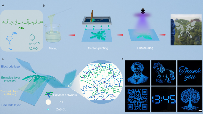
a Composition of the printable high-transparency, high-dielectric ink. b Flowchart illustrating the preparation process of the printed emissive layer. c Schematic diagram of the ACEL device structure. d Patterned electroluminescence achieved through screen printing of the ACEL devices. (Scale bar: 1 cm).
Characterization of the high-κ homogeneous printable ink
To ensure terminological clarity, we refer to the uncured transparent homogeneous liquid mixture of PUA/ACMO/PC as the dielectric ink, the UV-cured transparent gel as the dielectric gel, and the ZnS:Cu containing mixture used for emissive layer screen printing as the luminescent ink. By employing a small-molecule compound (PC) as the solvent in the homogeneous dielectric ink, we simultaneously enhance the dielectric constant and maintain high transmittance. Thanks to the excellent compatibility between PC and the polymer matrix, the homogeneous dielectric ink maintains a uniform and stable form even when penetrating the dense mesh layer during screen printing, enhancing the uniformity and clarity of the printed patterns. We evaluated the relationship between the dielectric properties and the PC content. As shown in Fig. 2a, the dielectric constant increases with the amount of PC added, reaching values greater than 20 over the frequency range of 1 kHz to 100 kHz when the PC weight fraction is 30%. This behavior can be interpreted using the classical Lichtenecker effective medium theory (Supplementary Fig. 6). However, as the PC content increases, the dielectric loss also gradually rises (Supplementary Fig. 7). This is attributed to the dipolar relaxation losses of the highly polar PC molecules, which undergo rotational and translational motion delays under alternating electric fields due to their small molecular nature. Furthermore, our investigation of the temperature effect on the dielectric properties revealed that both the dielectric constant and dielectric loss significantly increase with rising temperature (Supplementary Fig. 8). We further evaluated the mechanical properties of dielectric gels with different PC contents using tensile and compression tests (Fig. 2b, Supplementary Fig. 9). Increasing PC content resulted in a clear reduction in both maximum strain and tensile strength. Compression tests showed a significant decrease in compressive stress at the same strain levels, indicating reduced stiffness. This is primarily due to the plasticizing effect of PC, which reduces the crosslink density after UV curing and weakens the interactions between polymer chains, rendering the network softer and mechanically less robust. Owing to the excellent compatibility between the solvent PC and the transparent polymer matrix eliminating the need for refractive index matching, the resulting dielectric gel exhibits high transmittance, with up to 90 % transmittance in the visible light range, which remains high even after stretching (Fig. 2c). Differential scanning calorimetry (DSC) and thermogravimetric analysis (TGA) were performed on the cured dielectric gel (Fig. 2d, Supplementary Fig. 10). The DSC results show a glass transition temperature (Tg) of approximately −61.5 °C for the dielectric gel with 30 wt% PC, suggesting good flexibility at room temperature and below. The TGA curve indicates that the material remains thermally stable up to 120 °C, which is sufficient for ACEL operation. Rheological temperature sweep tests on the dielectric gel confirmed that the storage modulus (G′) remained higher than the loss modulus (G″) over the range from 25 °C to 200 °C, indicating complete transition from liquid to solid upon UV curing (Fig. 2e). Amplitude sweep and frequency sweep measurements (Supplementary Fig. 11) further reveal a distinct linear viscoelastic region (LVR) at small strains, with G′ consistently exceeding G″ across the entire strain and frequency range. These results confirm the formation of a stable, predominantly elastic 3D polymer network structure that supports high shape retention and robustness for printed dielectric layers. Compared with the dielectric layer materials for ACEL devices with screen-printing potential reported in previous studies, our developed dielectric gel exhibits a favorable combination of high-dielectric constant and high transmittance, as shown in Fig. 2f. In addition, leakage current measurements on the dielectric gel with 30 wt% PC (Supplementary Fig. 12) show low leakage levels under high electric fields, indicating good insulating performance.
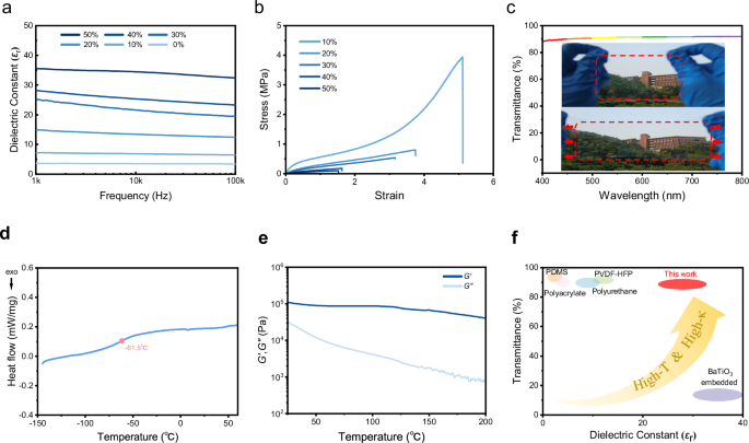
a Dielectric constants of dielectric gel with various PC contents. b Mechanical properties (tensile test) of dielectric gels with varying PC contents. c Transmittance measurement of dielectric gel with 30 wt% PC (thickness: 1 mm). d Differential scanning calorimetry (DSC) analysis of the dielectric gel with 30 wt% PC. e Rheological temperature sweep of the dielectric gel with 30 wt% PC after UV curing. G′ represents the storage modulus and G″ represents the loss modulus. f Comparison of dielectric constant and transmittance data of the developed dielectric gel with previously reported printable dielectric materials. (PDMS31, Polyacrylate42,43, polyurethane21,44, PVDF-HTP16,45, BaTiO34,7,34).
Exploration of printing performance
The viscosity of dielectric ink can be effectively regulated by adjusting the polymer matrix content and the amount of PC. We investigated the effect of PC content on dielectric ink viscosity. As shown in Fig. 3a, the viscosity of dielectric ink decreases significantly with increasing PC content. Simultaneously, the contact angle of dielectric ink on conductive glass also decreases as the PC content increases, which facilitates better adhesion of dielectric ink on the printing surface (Supplementary Fig. 13). To further analyze the rheological behavior, we used a rheometer to perform a steady-state flow step (SSFS) test on dielectric ink with 30 wt% PC content and on luminescent ink containing 200 wt% ZnS:Cu phosphors. As shown in Fig. 3b, the dielectric ink exhibits nearly constant viscosity with increasing shear rate, demonstrating Newtonian fluid-like behavior. In contrast, the luminescent ink exhibits higher viscosity at the same shear rate and shows shear-thinning behavior, indicating that its internal structure is more easily disrupted under shear. To systematically evaluate the influence of ZnS:Cu particles on the rheological behavior prior to UV curing, we performed amplitude sweep, frequency sweep, and shear rate sweep tests (Supplementary Fig. 14) on inks with and without phosphor particles. Amplitude sweep confirmed that both samples exhibit a phase angle δ close to 90°, with G″ significantly higher than G′, indicative of viscous liquid behavior. Frequency sweep further showed that both G′ and G″ increased with frequency, maintaining G″ > G′ across the range, confirming viscoelastic liquid behavior. The presence of phosphors did not alter the dominance of viscous response. To simulate the screen-printing process, a three-step peak hold step (PHS) test was conducted (Supplementary Fig. 15): (i) Low shear rate (0.1 s⁻¹ for 90 s), mimicking pre-print rest; (ii) High shear rate (1000 s−¹ for 30 s), mimicking squeegee motion; (iii) Return to low shear (0.1 s−¹ for 120 s), assessing structure recovery. The luminescent ink showed high and stable viscosity during rest, a sharp viscosity drop during shear (favorable for mesh penetration), and rapid viscosity recovery afterward, demonstrating excellent shear-thinning and self-recovery properties. These are essential for high-resolution printing with minimal pattern distortion. Figure 3c presents photographs of the ink before and after the addition of ZnS:Cu. Since ZnS:Cu does not dissolve in the ink but forms a suspension, sedimentation inevitably occurs over time. According to Stokes’ law, the sedimentation rate decreases with increasing viscosity. For luminescent ink with 30 wt% PC, sedimentation becomes apparent only after 5 hours of resting (Supplementary Fig. 16). Given our UV curing process solidifies the luminescent ink within ~30 s post-printing, the pigment is rapidly immobilized, and sedimentation does not impact pattern quality or industrial application. The screen-printing process is illustrated in Fig. 3d and can be broadly divided into four stages:(i) The luminescent ink uniformly fills the mesh holes and accumulates on one side of the screen; (ii–iii) The squeegee presses down and moves to the other side, bringing the screen into contact with the substrate. Under the applied pressure, the luminescent ink passes through the mesh and transfers to the substrate; (iv) Upon completing the print, the squeegee is lifted vertically, releasing the printing pressure. The screen separates from the substrate, leaving the luminescent ink fully transferred; (v) The luminescent ink spreads smoothly on the substrate surface. To ensure the clarity of printed patterns, we investigated the effects of luminescent ink viscosity (mass fraction of PC) and screen mesh size on the printing quality. Mesh count refers to the number of mesh holes per inch: 100, 200, and 300 mesh correspond to approximate openings of 150 μm, 74 μm, and 48 μm, respectively (minor variation depending on fiber diameter). Micrographs of these meshes are shown in Supplementary Fig. 17. Using luminescent ink with 30 wt% PC, we printed patterns with screens of 100, 200, and 300 mesh sizes and examined the central and edge regions under a microscope (Fig. 3e). For the 100-mesh screen, large mesh openings allow excessive luminescent ink flow, causing blurry edges and low resolution. The 300-mesh screen has openings similar to the size of ZnS:Cu ( ~ 25 μm), which leads to blockage and incomplete transfer. The 200-mesh screen achieves optimal balance with clear pattern edges and uniform transfer.
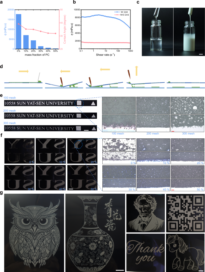
a Viscosity and contact angle of dielectric inks with different PC contents at room temperature, each bar chart column represents a single measurement. b Viscosity variation of the dielectric ink (without ZnS:Cu) and luminescent ink (with ZnS:Cu) containing 30 wt% PC with increasing shear rate. c Photographs of the dielectric inks before (left) and the luminescent ink after (right) the addition of electroluminescent powder (ZnS:Cu) (scale bar: 1 cm). d Schematic illustration of different stages of the screen-printing process. e Effect of luminescent ink viscosity on printing quality (scale bar: left,1 cm; right,200 μm). f Influence of screen mesh size on printing quality (scale bar: left,1 cm; right,200 μm). g Demonstration of printed luminescent patterns (scale bar: left,5 cm; right,1 cm).
According to the Hagen–Poiseuille law:
$$Q=\frac{\uppi \cdot {D}^{4}\cdot \,\Delta p}{128{{\eta }}L}$$
(1)
where Q is the ink volume flow rate, D is mesh opening diameter, η is viscosity, L is mesh thickness, and Δp is pressure. When viscosity is constant, mesh size D determines ink volume transfer. Oversized mesh allows over-flowing and blurred edges, while too-small mesh restricts transfer. Thus, the 200-mesh screen was chosen. Fig. 3ef shows the effect of luminescent ink viscosity (PC content ranging from 0 wt% to 50 wt%) on printing quality. luminescent inks with 0 wt%, 10 wt%, and 20 wt% PC content exhibited uneven particle distribution or unclear boundaries. However, excessive PC increases dielectric loss and softens the polymer network, compromising performance. Based on viscosity, dielectric loss, mechanical properties, and printability, we selected 30 wt% PC luminescent ink for further use. To demonstrate the printing capabilities, we printed a variety of complex patterns (Fig. 3g) with clear and uniform results, showcasing the luminescent ink’s excellent printability. To assess resolution, we printed features with line widths ranging from 50 to 600 μm (Supplementary Fig. 18). A minimum feature size of ~100 μm was achieved, satisfying high-resolution needs in flexible electroluminescent devices. We compared this with previously reported high-k patterned ZnS:Cu ACEL devices and summarized their patterning methods, resolution, and dielectric fillers (Supplementary Table 1). In addition to ITO-PET, we printed on FTO glass, conductive fabrics, and stainless steel substrates (Supplementary Fig. 19), all yielding sharp patterns, confirming the luminescent ink’s substrate versatility. Contact angle and surface energy measurements (Supplementary Tables 2 and 3) indicate that ITO-PET, FTO, and 304 stainless steel have higher surface energy than conductive fabric. The screen mesh (PET, ~42 mN/m) has slightly lower surface energy than that of most substrates, which aids in luminescent ink transfer and resolution. Finally, adhesion between cured luminescent ink layers and ITO-PET electrodes was evaluated via cross-cut adhesion test (ASTM D3359). Both dielectric and emissive layers achieved 4B rating, demonstrating strong adhesion (Supplementary Fig. 20).
Investigation of ACEL device performance
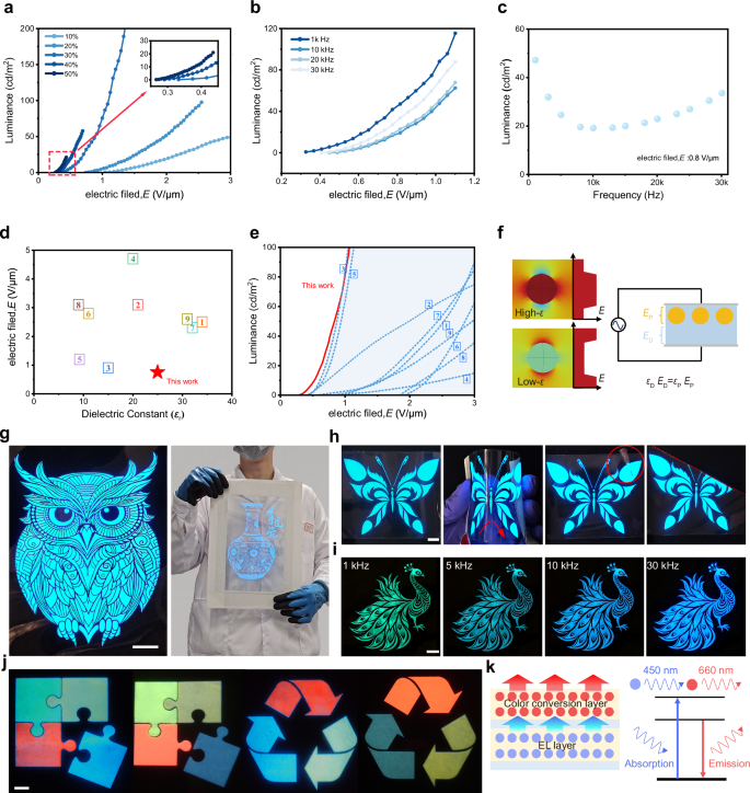
We conducted luminescence performance tests of ACEL devices (Supplementary Fig. 21). Under a 1 kHz sinusoidal voltage, the relationship between luminance and electric field strength for devices with different PC contents is shown in Fig. 4a. As the PC content increased from 10 wt% to 50 wt%, the device luminance significantly improved under the same electric field, while the required driving voltage decreased. However, excessive PC content (>40 wt%) led to severe device heating due to increased dielectric loss, limiting the maximum applicable voltage. Compared with devices using different dielectric materials, PC-containing devices showed substantial luminance enhancement, Supplementary Fig. 21, and the device using 30 wt% PC dielectric ink achieved a driving voltage as low as ~0.33 V/μm. We measured the luminance at frequency ranging from 1 kHz to 30 kHz (Fig. 4b, c). In addition, Supplementary Fig. 23 presents the relationship between actual applied voltage and luminance. The device exhibited maximum luminance at 1 kHz, which gradually decreased with increasing frequency, reaching a minimum around 10 kHz, and then increased with further frequency elevation. This behavior deviates from the monotonic increase commonly reported in previous studies. The underlying mechanism remains unclear but is likely associated with the characteristic frequency response of the dielectric matrix used in this work. Compared with previously reported ACEL devices, our approach exhibits enhanced performance in terms of luminance and driving voltage (Fig. 4d, e and Supplementary Table 4). This improvement is due to the uniform enhancement of the dielectric constant throughout the matrix by PC addition, which enhances the electric field experienced by the phosphors. COMSOL simulation results support this finding (Fig. 4f). Supplementary Fig. 924 compares simulations using commonly used PDMS and BaTiO₃-doped PDMS as dielectric media. Pure PDMS, with its low dielectric constant (~3), limits the electric field experienced by the phosphor, thereby restricting luminance performance. Incorporating high-dielectric-constant ceramic fillers like BaTiO₃ can reduce their own voltage drop, allowing more voltage to be applied across the phosphor particles. However, achieving this requires substantial filler content, occupying a significant volume of the matrix (Supplementary Fig. 24a). Due to their inherent opacity, these fillers can hinder light transmission, affecting luminance efficiency. This phenomenon explains why many BaTiO₃-enhanced ACEL devices exhibit limited luminance improvement despite high-dielectric constants, as shown in Fig. 4d (samples  ,
,  , and
, and  ). A microscopic cross-sectional image of our ACEL device is shown in Supplementary Fig. 25, confirming its layered structure. The ink developed in this study achieves high luminance and low driving voltage, providing substantial potential for multidimensional applications of EL devices in emerging areas. We fabricated large-area ACEL devices in the laboratory, as demonstrated in Fig. 4g, indicating the feasibility of large-scale industrial production. Figure 4h showcases the device’s flexibility, including bending, piercing, and cutting capabilities. Due to the characteristics of the phosphor, the emission color of the device shifts under different applied electric field frequency. As shown in Fig. 4i, increasing the frequency causes a blue shift in the emission color (from green to deep blue). We combined this property with signal modulation; by amplifying specific modulation signals through a power amplifier and applying them to the EL device, controllable color-changing emission was achieved (Supplementary Movie 1). Due to the intrinsic properties of the phosphors, the emitted light is limited to the blue-green range. To achieve a wider variety of colors, we applied inorganic fluorescent powders with different emission wavelengths as color conversion layers on the device surface. These inorganic fluorescent powders can absorb light within the 300 nm to 500 nm range, allowing them to absorb the blue-green light emitted by the ZnS:Cu layer and re-emit light in different colors, as shown in Fig. 4k. For this purpose, we selected three types of inorganic fluorescent powders (Supplementary Fig. 26) with emission wavelengths of 660 nm (red), 558 nm (yellow), and 518 nm (green) to fabricate multicolor electroluminescent devices, as shown in Fig. 4j. The use of inorganic fluorescent powders effectively addresses the issue of photodegradation commonly observed in organic fluorescent materials, significantly enhancing the durability and stability of the color conversion layer. In contrast, organic phosphors are prone to photobleaching, loss of emission efficiency, and color fading under prolonged UV irradiation and electric field exposure, due to photooxidation and bond breakage1.
Body-coupled enables wireless touch light-emitting device
Conventional touch-activated electroluminescent devices typically rely on wired power sources or triboelectric mechanisms, which suffer from structural complexity, high environmental dependency, and poor emission stability. The ink we developed successfully addresses these issues. Its high-dielectric constant facilitates the efficient utilization of ambient electromagnetic energy, while its screen-printable nature enables precise patterning of the luminescent layer, providing a key material foundation for the development of wireless smart interactive devices. We have designed and fabricated a wireless touch-activated luminescent device that collects ambient electromagnetic energy and then forms a closed energy loop through the human body and the ground to emit light (Fig. 5a, Supplementary Fig. 27). Structurally, the device comprises three layers from bottom to top: an antenna layer (ITO-PET) that senses alternating electromagnetic fields; an optical layer (ZnS:Cu mixed dielectric ink prepared via screen printing) that provides visual light information; and a dielectric layer (dielectric ink) that stores coupled electromagnetic energy. When the dielectric layer is touched by a human, an interfacial contact capacitance is formed, which excites the luminescent layer to emit visible light. This enables wireless touch-induced luminescence without the need for traditional power connections (Fig. 5b). Supplementary Movie 2 demonstrates that finger touches and slides emit light when wirelessly powered on, but not when wirelessly powered off, confirming that the luminescence results from human-coupled wireless electromagnetic energy rather than triboluminescence. As the distance between human skin and the dielectric layer decreases, the electric field intensity between them gradually increases. When it exceeds the critical value for air breakdown, localized plasma discharge occurs, with ions and electrons rapidly colliding and migrating among air molecules in the gap (Fig. 5c). With further proximity, when the electric field surpasses the critical intensity of the luminescent material, doped carriers are excited to the conduction band and subsequently recombine with holes to emit visible light (Supplementary Movie 3). Utilizing the high-dielectric properties and printability of the ink, we can create optical layers with specific patterns through screen printing. These two-dimensional optical layers facilitate information display and transmission. As shown in Fig. 5d, e, we have developed a fingerprint collector and a touch luminescent keyboard, which show great innovative application prospects in fingerprint optical recognition and sensing as well as barrier-free information communication for deaf and mute people (Supplementary Movies 4 and 5). Fingerprints are essentially the raised ridges on the epidermis. When touching a surface, the height differences between these ridges and the surrounding skin allow the fingerprint patterns to become visible (as illustrated in Fig. 5a). The touch-activated luminescent keyboard is created by screen-printing letter patterns onto the luminescent layer, causing the corresponding letter to illuminate upon touch.
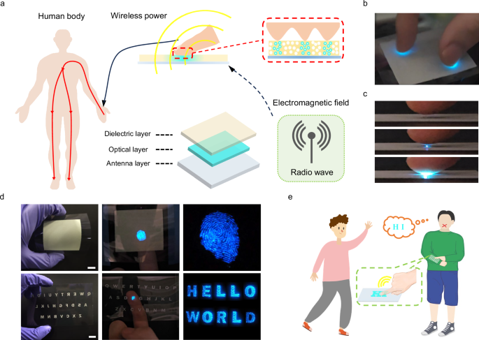
a Schematic diagram of wireless touch light-emitting device structure and light-emitting principle. b, c Demonstration of wireless touch-induced luminescence. d Display of fingerprint and textual information through wireless touch-induced luminescence (scale bar: 1 cm). e Potential application in providing auxiliary optical communication for individuals with deaf and mute.


3 Comments
https://shorturl.fm/wjKeW
https://shorturl.fm/7R5K2
https://shorturl.fm/zzPiu